

HY5DU121622CTP-D43
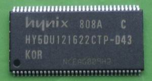
HY5DU121622CTP-D43
HY5DU121622DTP 资料标题简介
512Mb DDR SDRAM
HY5DU121622DTP 资料关键信息
• VDD, VDDQ= 2.3V min ~ 2.7V max
(Typical 2.5V Operation +/- 0.2V for DDR266, 333)
• VDD, VDDQ= 2.4V min ~ 2.7V max
(Typical 2.6V Operation +0.1/- 0.2V for DDR400
product )
• All inputs and outputs are compatible with SSTL_2
interface
• Fully differential clock inputs (CK, /CK) operation
• Double data rate interface
• Source synchronous - data transaction aligned to
bidirectional data strobe (DQS)
• x16 device has two bytewide data strobes (UDQS,
LDQS) per each x8 I/O
• Data outputs on DQS edges when read (edged DQ)
Data inputs on DQS centers when write (centered
DQ)
• On chip DLL align DQ and DQS transition with CK
transition
• DM mask write data-in at the both rising and falling
edges of the data strobe
• All addresses and control inputs except data, data
strobes and data masks latched on the rising edges
of the clock
• Programmable CAS latency 2/2.5 (DDR266, 333)
and 3 (DDR400 product) supported
• Programmable burst length 2/4/8 with both sequen-
tial and interleave mode
• Internal four bank operations with single pulsed
/RAS
• Auto refresh and self refresh supported
• tRASlock out function supported
• 8192refresh cycles/64ms
• JEDEC standard 400mil 66pin TSOP-II with 0.65mm
pin pitch
• Lead free (*ROHS Compliant)